
Author Affiliations
Abstract
1 School of Optical and Electronic Information, Huazhong University of Science and Technology, Wuhan 430074, China
2 Department of Applied Physics, KTH Royal Institute of Technology, Stockholm 11419, Sweden
3 Wuhan National Laboratory for Optoelectronics, Wuhan 430074, China
A novel power-efficient reconfigurable mode converter is proposed and experimentally demonstrated based on cross-connected symmetric Y-junctions assisted by thermo-optic phase shifters on a silicon-on-insulator platform. Instead of using conventional Y-junctions, subwavelength symmetric Y-junctions are utilized to enhance the mode splitting ability. The reconfigurable functionality can be realized by controlling the induced phase differences. Benefited from the cross-connected scheme, the number of heating electrodes can be effectively reduced, while the performance of the device is maintained. With only one-step etching, our fabricated device shows the average insertion losses and cross talks are less than 2.45 and , respectively, measured with conversions between two arbitrary compositions of the first four TE modes over an observable 60 nm bandwidth. The converter is switchable and CMOS-compatible, and could be extended for more modes; hence, it can be potentially deployed for advanced and flexible mode multiplexing optical networks-on-chip.
Photonics Research
2021, 9(1): 01000043

Author Affiliations
Abstract
1 School of Optical and Electronic Information, Huazhong University of Science and Technology, Wuhan 430074, China
2 Wuhan National Laboratory for Optoelectronics, Wuhan 430074, China
A high-efficiency inverse design of “digital” subwavelength nanophotonic devices using the adjoint method is proposed. We design a single-mode 3 dB power divider and a dual-mode demultiplexer to demonstrate the efficiency of the proposed inverse design approach, called the digitized adjoint method, for single- and dual-object optimization, respectively. The optimization comprises three stages: 1) continuous variation for an “analog” pattern; 2) forced permittivity biasing for a “quasi-digital” pattern; and 3) a multilevel digital pattern. Compared with the conventional brute-force method, the proposed method can improve design efficiency by about five times, and the performance optimization can reach approximately the same level. The method takes advantages of adjoint sensitivity analysis and digital subwavelength structure and creates a new way for the efficient and high-performance design of compact digital subwavelength nanophotonic devices, which could overcome the efficiency bottleneck of the brute-force method, which is restricted by the number of pixels of a digital pattern, and improve the device performance by extending a conventional binary pattern to a multilevel one.
Photonics Research
2020, 8(4): 04000528
Author Affiliations
Abstract
1 School of Electronic Information and Communications, Huazhong University of Science and Technology, Wuhan 430074, China
2 Wuhan National Laboratory for Optoelectronics and School of Optical and Electronic Information, Huazhong University of Science and Technology, Wuhan 430074, China
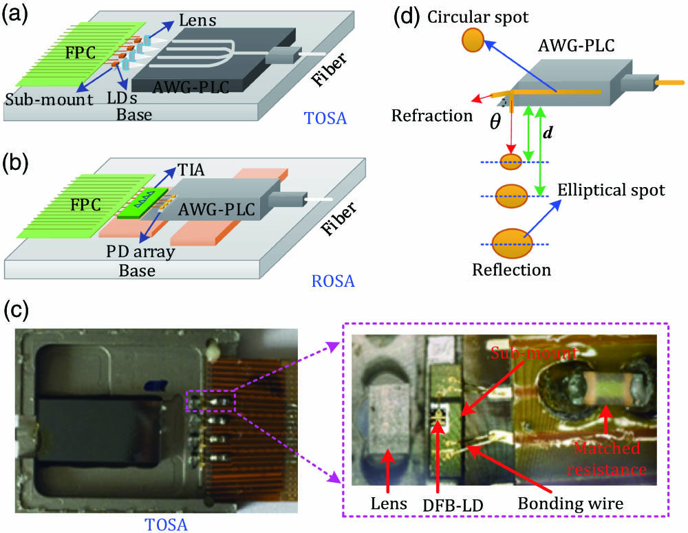
In this paper, an integrated compact four-channel directly modulated analog optical transceiver is proposed and fabricated. The 3 dB bandwidth of this optical transceiver exceeds 20 GHz, and the measured spurious-free dynamic range is up to . The optical coupling efficiency (CE) is improved by using a precise submicron alignment technique for lens coupling in a transmitter optical subassembly, and the highest CE is achieved when the oblique angle of the arrayed waveguide grating using a silica-based planar lightwave circuit (AWG-PLC) in receiver optical sub assembly is set to 42°. Based on the proposed optical transceiver, we have experimentally demonstrated a 6.624 Gbit/s multi-input multioutput (MIMO) 16-quadrature amplitude modulation orthogonal frequency division multiplexing (16QAM-OFDM) radio signal over 15.5 km standard single mode fiber, together with 1.2 m wireless transmission in both an uplink and a downlink. To cope with the channel interference and noise of the fiber-wireless transmission system, a low-complexity MIMO demodulation algorithm based on lattice reduction zero-forcing (LR-ZF) is designed. In our experiment, 1.6 dB power penalty is achieved by using the proposed LR-ZF algorithm, compared to the commonly used zero-forcing algorithm. Moreover, this LR-ZF algorithm has much less complexity than the optimal maximum-likelihood sequence estimation (MLSE) at a given transmission performance. These results not only demonstrate the feasibility of the integrated optical transceiver for MIMO fiber-wireless application but also validate that the proposed LR-ZF algorithm is effective to eliminate the interference for hybrid fiber-wireless transmission.
Photonics Research
2019, 7(12): 12001461

Author Affiliations
Abstract
School of Optical and Electrical Information, Huazhong University of Science and Technology, Wuhan 430074, China
With the rapidly increasing bandwidth requirements of optical communication networks, compact and low-cost large-scale optical switches become necessary. Silicon photonics is a promising technology due to its small footprint, cost competitiveness, and high bandwidth density. In this paper, we demonstrate a 12×12 silicon wavelength routing switch employing cascaded arrayed waveguide gratings (AWGs) connected by a silicon waveguide interconnection network on a single chip. We optimize the connecting strategy of the crossing structure to reduce the switch’s footprint. We develop an algorithm based on minimum standard deviation to minimize the port-to-port insertion loss (IL) fluctuation of the switch globally. The simulated port-to-port IL fluctuation decreases by about 3 dB compared with that of the conventional one. The average measured port-to-port IL is 13.03 dB, with a standard deviation of 0.78 dB and a fluctuation of 2.39 dB. The device can be used for wide applications in core networks and data centers.
Networks, wavelength routing Integrated optics devices Wavelength filtering devices Photonics Research
2018, 6(5): 05000380

Author Affiliations
Abstract
1 School of Optical and Electrical Information, Huazhong University of Science and Technology, Wuhan 430074, China
2 Wuhan National Laboratory for Optoelectronics, Huazhong University of Science and Technology, Wuhan 430074, China
We propose and experimentally demonstrate a novel ultracompact dual-mode waveguide crossing based on subwavelength multimode-interference couplers for a densely integrated on-chip mode-division multiplexing system. By engineering the lateral-cladding material index and manipulating phase profiles of light at the nanoscale using an improved inverse design method, a subwavelength structure could theoretically realize the identical beat length for both TE0 and TE1, which can reduce the scale of the device greatly. The fabricated device occupied a footprint of only 4.8 μm×4.8 μm. The measured insertion losses and crosstalks were less than 0.6 dB and 24 dB from 1530 nm to 1590 nm for both TE0 and TE1 modes, respectively. Furthermore, our scheme could also be expanded to design waveguide crossings that support more modes.
Integrated optics devices Multiplexing Metamaterials Photonics Research
2018, 6(7): 07000660
School of Optical and Electronic Information, Huazhong University of Science and Technology, Wuhan 430074, China
Frontiers of Optoelectronics
2016, 9(4): 571–577
1 School of Optical and Electronic Information, Huazhong University of Science and Technology, Wuhan 430074, China
2 Wuhan National Laboratory for Optoelectronics, Huazhong University of Science and Technology, Wuhan 430074, China
A highly efficient tunable optical filter of liquid crystal (LC) optical micro-ring resonator (MRR) was proposed. The 4-μm-radius ring consists of a silicon-oninsulator (SOI) asymmetric bent slot waveguide with a LC cladding. The geometry of the slot waveguide resulted in the strong electro-optic effect of the LC, and therefore induced an increase in effective refractive index by 0.0720 for the quasi-TE mode light in the slot-waveguide. The ultra-wide tuning range (56.0 nm) and large free spectral range (FSR) (~28.0 nm) of the optical filters enabled wavelength reconfigurable multiplexing devices with a drive voltage of only 5 V. The influences of parameters, such as the slot width, total width of Si rails and slot shift on the device’s performance, were analyzed and the optimal design was given. Moreover, the influence of fabrication tolerances and the loss of device were both investigated. Compared with state-of-the-art tunable MRRs, the proposed electrically tunable micro-ring resonator owns the excellent features of wider tuning ranges, larger FSRs and ultralow voltages.
integrated optics devices integrated optics devices liquid crystals liquid crystals micro-ring resonator micro-ring resonator slot waveguide slot waveguide wavelength tuning wavelength tuning Frontiers of Optoelectronics
2016, 9(1): 112
1 华中科技大学 光学与电子信息学院, 武汉 430074
2 烽火通信科技股份有限公司, 武汉 430073
基于微环谐振腔FWM(四波混频)效应产生的OFC(光频梳)可实现多波长光源和光孤子传输、存储等, 能很好地满足光通信网络的要求。对基于微环谐振腔的OFC已有大量的实验报道, 但是理论研究却有些不足。文章介绍了目前两种微环谐振腔OFC的理论分析方法, 即NCME(非线性耦合模方程)和非线性LLE (Lugiato-Lefever方程), 对这两种方法的优缺点进行了比较分析。结果表明, LLE由于其计算速度快, 更适合用于基于微环谐振腔的超宽带OFC的理论研究。
微环谐振腔 四波混频 光频梳 非线性耦合模方程 非线性Lugiato-Lefever方程 micro-ring resonator FWM OFC NCME nonlinear LLE
National Engineering Laboratory for Next Generation Internet Access System, Huazhong University of Science and Technology, Wuhan 430074, China
Frontiers of Optoelectronics
2014, 7(4): 493–500
1 华中科技大学 光学与电子信息学院, 湖北 武汉430074
2 烽火通信科技股份有限公司, 湖北 武汉430074
当前以电子作为信息载体的微电子技术遭遇到发展瓶颈。光传输具有带宽大、速率高的特点, 将光子载体与电子载体相结合是未来信息传输发展的必然趋势。波导与光纤的高效耦合是实现光电子集成的关键。文章介绍了国内外几种典型耦合器的最新进展, 包括楔形耦合器、GRIN(渐变折射率)透镜耦合器和垂直光栅耦合器, 并对它们的性能指标、优缺点进行了比较分析, 对进一步提高耦合效率的可行性进行了展望。结果表明, 垂直光栅耦合器具有耦合效率高、带宽大、工艺成熟、工艺容差大和耦合步骤简单的优势, 在光通信与集成光电子学领域有着广阔的应用前景。
硅基光子学 耦合器 耦合效率 silicon-based photonics coupler coupling efficiency


